We broadly interested in novel medical imaging technologies, for now, we have two main research focuses:


Here are some research topic we also interested about:
- Digital Radiological Imaging Detectors
- Single Photon Counting for Medical Imaging
- Detector Modeling, Fabrication, Characterization and Instrumentation
- Avalanche Amorphous Selenium Detectors
- Quantum Mechanical Modeling of Charge Transport
Research Highlights:
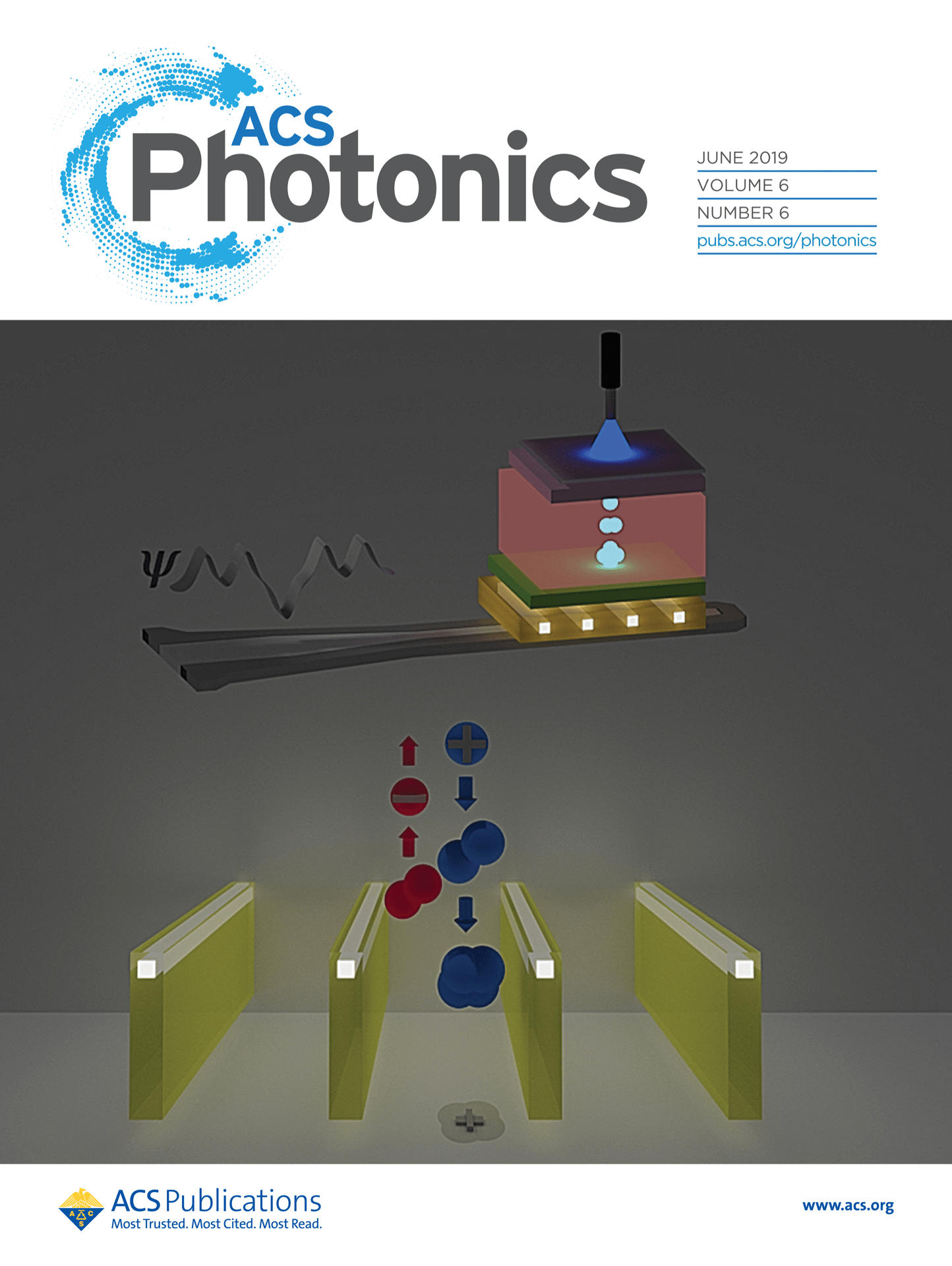
- Picosecond timing in an avalanche amorphous selenium semiconductor is achieved by implementing Nano-Frisch grids along the collecting electrode to form a multiwell structure. The induced photocurrent following optical impulse exposure is independent of carrier motion outside the wells resulting in unipolar time-differential charge sensing via extended-state hot hole transport. This is the first experimental report of avalanche gain and picosecond time-resolution using an amorphous semiconductor. Further analysis suggests we may be able to achieve sub-100 picosecond coincidence timing resolution in time-of-flight PET using our multiwell selenium semiconductor as the photodetector.

For more information, please click here and here.
- I have been working on the development of large-area avalanche x-ray detectors for more than 10 years. I have extensive experience in the development and fabrication of amorphous selenium (a-Se) radiation detectors, and performed instrumental research work that led to the development of the first ultra-fast field shaping amorphous detector. I have co-invented, developed and optimized a number of different direct and indirect detector technologies. My most significant contribution to research is introducing the novel concept of unipolar time-differential (UTD) charge sensing in amorphous solids using a field shaping multi-well detector structure. This feature enables amorphous detectors to operate at their theoretical limit of charge diffusion and improves their time-resolution by multiple orders-of-magnitude. I also designed, fabricated, and tested the first field shaping a-Se UTD device using the proposed multi-well structure and demonstrated 300-times better time-resolution. A US patent was awarded to this new technology and the 16-page publication in the journal of applied physics appeared on the cover of vol. 113, issue 22.

For more information, please click here.
- Amorphous selenium (a-Se), in the form of thermally deposited thin films, is the only x-ray photoconductor that has been successfully developed for making large area medical image sensors. It’s also the only amorphous material that has avalanche multiplication gain. I simulated a nanopattern multi-well a-Se detector, called NEW-HARP, to enable the utilization of both avalanche multiplication gain and UTD charge sensing in one device. I showed that, for a-Se operating in the avalanche mode at high electric fields, charge drift occurs via band transport in extended states with non-activated microscopic mobility, and thus, photocarriers experience negligible interruption by capture and thermal-release events due to shallow traps. The implication of (1) non-activated microscopic band-mobility, (2) avalanche gain, and (3) UTD charge sensing is the realization of a photodetetctor that can achieve < 100 ps time-resolution with a material that is low-cost and uniformly scalable to large-area. The realization of the proposed NEW-HARP would be a great leap forward in radiation detection with applications not only in medical imaging (such as Time-Of-Flight PET), but also in particle physics (such as Cherenkov imaging detectors and trackers), optical communication, and time-domain spectroscopy.
- I have also made major contribution to the fundamental understanding of amorphous selenium. In collaborating with Oak Ridge National Lab (US), Brookhaven National Lab (US), and Quantum Wise (Denmark), I resolved the long-lasting controversy concerning the molecular structure of amorphous selenium by showing that the structures of vapor- and melt-quenched amorphous selenium are quite different, based primarily on rings and chains, respectively, reflecting the predominant structure of the parent phase in thermodynamic equilibrium. The result of this work helped fill the gap in understanding the link between the microscopic molecular structure and other macroscopic observable phenomena (such as avalanche transport and material stability/crystallization) which was hindering the development of (1) fundamental frameworks for transport and structural studies and (2) interface blocking layers to enable reliable and repeatable impact ionization gain in these avalanche devices.

For more information, please click here.
Grants:
- 2020, NIH REACH POC (funded), PI: “Development of an ultra-high resolution Brain PET.”
- 2019, NIH R01 (funded), PI: “SWAD: Large-Area Photon Counting X-Ray Imager using Amorphous Selenium,” ranked 10th percentile.
- 2018, NIH R01 (funded), Co-I: “BI-SHARP-AMFPI: high frame-rate and low-dose x-ray,” ranked 4th percentile.
- 2018, NIH R21 (funded), PI: “Field Shaping SHARP-AMFPI: Towards Large-Area, High-Efficiency, and Low-Dose X-ray Imaging,” ranked 14th percentile.
- 2017, NIH R21 (funded), PI: “Se-SSPM: Towards a Low-Cost MR-Compatible Time-Of-Flight PET,” ranked 6th percentile.
- 2017, NIH REACH POC (funded), PI: “Selenium Multi-Well Avalanche Detector for Medical Imaging Applications: mammography and Time-Of-Flight PET.”
- 2016, NIH REACH POC (funded), PI: “NEW-HARP: A highly sensitive avalanche selenium detector for time-of-flight (TOF) positron emission tomography (PET).”
- 2015, NIH R21 (funded), Co-I: “SWAD: Towards Photon Counting Using Amorphous.”
- 2014, SBU-BNL SEED (funded), PI: “Molecular Structure of Thin-Film Amorphous Selenium.”